
Porous Films with Low Dielectric Permittivity
Description
The new technology is designed to be used in manufacturing of microwave electronics and is unique in that it offers a simple method for manufacture of porous dielectric layers. An important aspect of the technology is that it is implemented in vacuum, which makes it fully compatible with methods for manufacture of individual IC elements.
Specifications
- Thickness: 20 to 500 nm
- Allows controllable adjustment of dielectric permittivity
- Allows controllable adjustment of pore density and size
Advantages
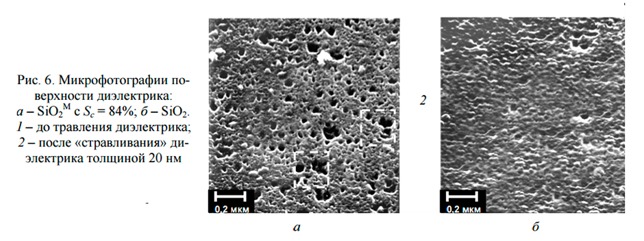
The technology makes use of a new approach to formation of porous film dielectrics: modification by injection of carbon. Underlying the technology is the vacuum method for silicon dioxide dielectric film formation by sputtering of a composite silicon-carbon target in magnetron discharge plasma in the atmosphere of the plasma-forming gas. Physico-chemical processes that take place on the base material create a meso- and macroporous dielectric film of silicon dioxide with a pre-defined size and density of pores.
Application
Manufacturers of microwave ICs, gas-sensing probes and sensors. Nanoelectronics engineering.